Advantages of HDI PCBs
HDI PCBs
The main advantage of HDI PCBs is that they allow more circuitry to be packed into smaller spaces. They can be used in handheld devices, medical equipment and other gadgets that require minimal space. They can also be incorporated in industrial machinery that is becoming more computerized.
These high-density interconnector circuit boards are also more durable than standard PCBs. They can withstand harsh weather conditions, and their layers are more tightly bonded together. This reduces the chances of failure caused by thermal shock or accelerated thermal cycles. In addition to their durability, hdi pcb circuit boards use less power than standard PCBs, which can help extend battery life on handheld devices and other electronics.
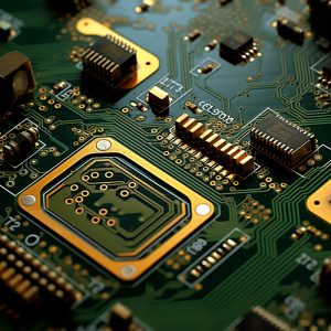
Manufacturers use three techniques to build HDI circuit boards: stacked vias, blind and buried vias, and the via-in-pad process. Using these processes, manufacturers can place components closer to each other, which can reduce the size of a circuit board by up to 40%. They can even fit more components on a single side of a circuit board. This can make the device more portable and increase its functionality.
Advantages of HDI PCBs
Several factors can affect the cost of an HDI PCB, including the number and type of vias, through-holes, or microvias, the stackup height, and the number of sequential laminations. The cost can also be impacted by the choice of materials, including core or base and surface finish. For example, the core or base material may be metal or fiberglass, while the surface finish can be ENIG, HASL, immersion tin, immersion silver, gold, and more. Choosing the right surface finish can save money on the assembly process because it is easier to solder.
The via-in-pad process allows manufacturers to place a via on a flat land on an HDI PCB by plating it, filling it with one of many different fill types, capping it, and then plating over it. This is a complex process that requires skilled workers and special tools, but it can help reduce the size of a circuit board by reducing its overall footprint. It can also simplify thermal management and provide one of the shortest routes to bypass capacitors in high-frequency layout designs.
Another major benefit of HDI PCBs is their improved signal quality. The reduced distance between components means that signals can travel quickly, with less noise and cross-talk. This can improve the performance of a device or machine, and it can also lead to lower power consumption, which is good for the environment.
There are many other advantages of HDI PCBs, but they can be hard to see if you don’t have the right understanding of how they work. The key is to plan your orders well in advance and to choose a reliable supplier that can offer fast turnaround time. This will ensure that you can meet your deadlines and keep your project running smoothly. Besides, a good supplier will be able to provide you with the best possible customer service and support.